A number of people have contacted me by email, after seeing the PCB quality displayed on my height Probing with pcb-gcode page, and complain about the quality of their own PCBs.
The number one problem I see, is people not aware what size their routing bit actually is, and number two problem is unrealistic expectations.
When you use pcb-gcode to isolation-route your PCB's, you need to calibrate the width of the grove your bit routes in the copper layer, you need to enter this number in pcb-gcodes Etching Tool Size or pcb-gcode will produce wrong G-code.
You do not need to have access to a calibrated microscope, with some applied smartness, a regular flatbed scanner will do.
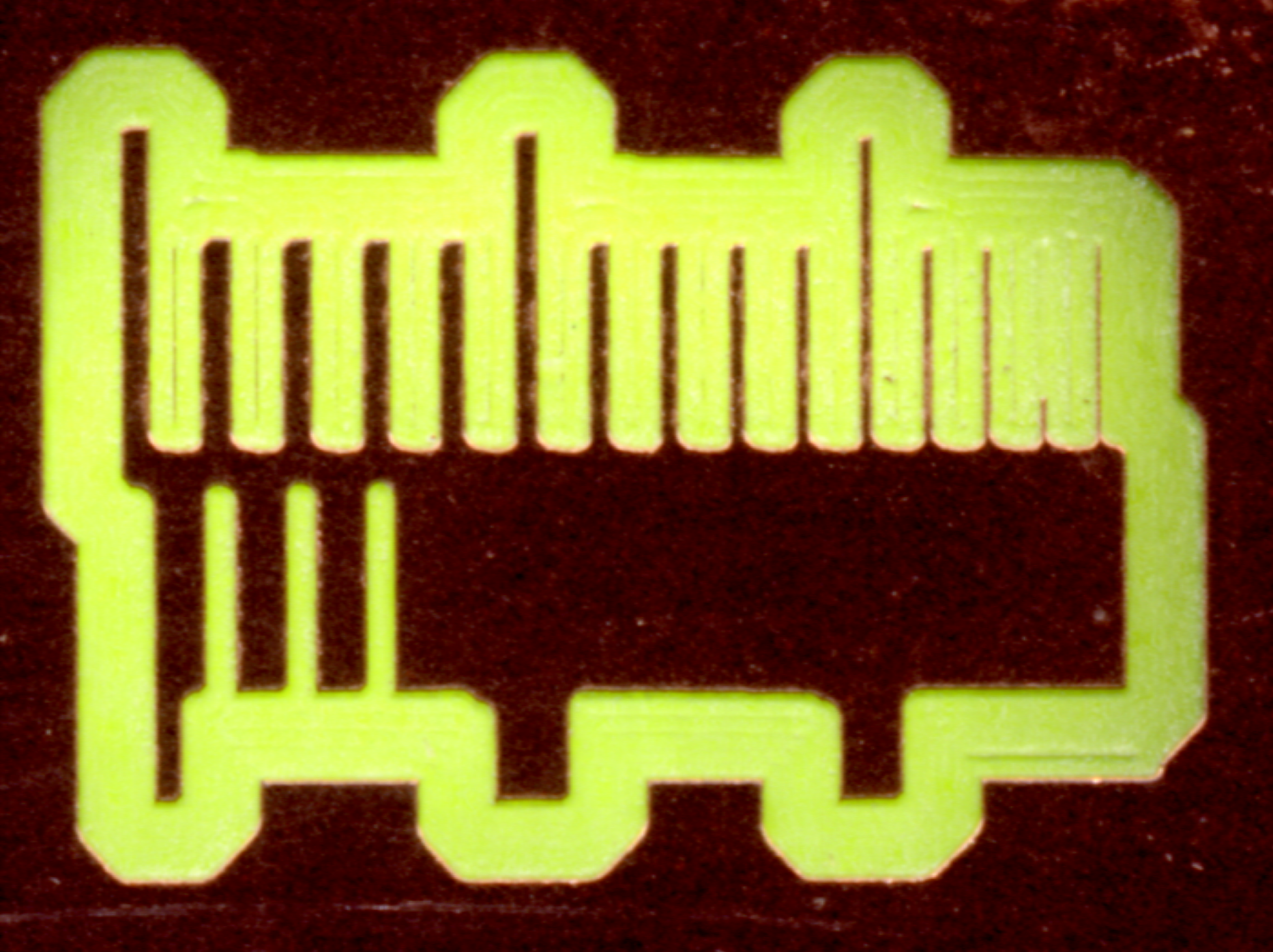
This is a scan of my test-pattern with a correctly calibrated bit: (Click on the picture to get the full sized version.)
I scanned this by putting the PCB on the flatbedscanner, covered the backside with a piece of regular white paper, and then balanced a LED-torchlight on top of the pattern, to illuminate the fibreglass substrate, and scanned it, at what my scanner claims is 3200DPI. Use your scanners preview/crop function to get a sensible filesize.
The testpattern consists of a number of wires and isolations of increasing width. In the top right in the picture above, you can see the 1mil width wire. (Yes, you read that right: that is a 1mil = 0.0254mm wire. Perfectly useless, but there, nontheless.)
Continuing left, the 2mil wire didn't survive, and the last one on the far left is 15mil wide. Notice that 5, 10, 15mil are slightly longer for orientation/counting convenience.
At the bottom you will notice that only the 12-15mil isolations have been attempted by pcb-gcode, because my bit is configured in pcb-gcode with a width of 0.3mm = 11.8mil.
So how does the test-pattern tell you that you have the right width ?
Simple: The isolations and the wires right above them should have the same width. If the isolation is wider than the wire, you bit is wider than you told pcb-gcode, if the wire is wider than the isolation, it is more pointed than you told pcb-gcode.
Depending on your level of ambition, you can just fix it up by eye or scan it on your flatbed and count pixels. Figure out the math yourself.
Once you have found the width, remember to set the "Step Size" in pcb-gcode to 30-50% of the width.
The calibration pattern is here, as an EagleCad script file, and as the Tcl script which generates it:
cal_pattern.scr cal_script.tclUse "save as" in your browser to save the cal_pattern.scr file locally, then in eagle type "SCRIPT cal_pattern.scr" in an empty PCB and you are all set. You can delete the edges you do not need, like I did above.
Unless you do some kind of height calibration/probing/floating-head, you are not likely to get performance anywhere close to what I have above.
The basic problem is that you are trying to remove 35 micrometer (1.4 mil) copper, from the top of 1.5mm (60mil) glasfiber-epoxy with a 10% thickness tolerance.
Even a CNC-rig with 1mil repeatable precision and a vacuum table cannot do anything about a copperlayer which surfs on 6 mil epoxy-waves. The only thing that works, is to route relative to the top-, rather than the bottom-surface of the PCB.
In general, the more wobbly your CNC rig is, the more a pointy bit will help you yout, due to the geometry. I use 60 degree V-bits, if that does not work for you, try 30 degree bits.
No, I have to tried to use 5mil traces.
Yet.
Thanks to John Johnson for the PCB-GCode program. It is a neat trick.
Poul-Henning