HP5065 Clock Upgrade
The LED clock in my HP5065A was very dim and even though I don’t particularly need another clock in my lab, it irritated me.
What irritated me more was that, seen from my point of view, quite a lot of the electronics in the HP5065A are only there to drive that clock.
First the A6 board divides 5 MHz directly from the secondary (“DIV”) OCXO output down to 1 MHz - for which I have no use.
The A4 board divides that further down to 100 kHz - for which I have even less use.
The A5 module takes the 1 MHz and divides it down to 1 Hz, possibly synchronizing it to an external SYNC input with some chosen number of microseconds offset.
A16 converts the old analog clock signals from A5 the new A19 LED clock module.
What makes all this “Surplus to requirements” hardware particularly annoying to me, is that you have to remove A5 and A16 if you want to adjust the A3 60 MHz Frequency Multiplier module.
So inspired by Tom Van Baak’s PPSDIV idea, I started a little X-Mas project to get rid of all this hardware which, as far as I care, just takes up space and power for no good reason.
Circuit Design
I first toyed with designing a new single board clock where the LED’s were driven directly by a microcontroller, but I realized that there were no way I could fit what I wanted, in particular the SYNC input and PPS output circuits, unless I went to SMD components I could not hand-solder.
Having resigned to a two-board design it was an obvious no-brainer to reuse the existing LED board, which works fine, my dim display is caused by the 5V switch-mode regulator for the LED driver.
I decided to use NXP’s cute little 8-pin ARM processor, the LPC810, because I’m sick and tried of crappy microcontrollers with arcane instruction sets, tiny registers and byzantine hardware architectures.
I found two cheap 78xx plug compatible switch-mode voltage regulators to supply 12V to the MM5313 chip on the A19A2 board, and 3.3V to the ARM and the LED drivers.
Originally the LED drivers got 5V, but 3.3V works fine and the slightly less blinding display works for me.
Total power consumption is just a tad over 1 Watt now.
I have put a a C-L-C filter on the power input, to make sure no noise from the two switches make it backwards.
The input 5 MHz clock signal is only 0.2 Vpp and is taken out before the output amplifier in the OCXO. That worries me a bit from a noise perspective, but if that transpires to be an issue, the solution is trivial: Take the 5MHz from the A13 buffer amplifier instead.
Based on advice from Attila Kinali on the time-nuts mailing list, I decided to use a TLV3501 comparator to make 3.3V CMOS squares out of the 5 MHz signal.
As mentioned I wanted to retain the HP5065A’s ability to sync to external PPS signals and also to generate a PPS output.
Both of those signals are protected by diodes to the power rails.
I did consider adding a RTC clock, but decided against it.
First because I don’t intend to turn the HP5065 on and off a lot, so it would be hardly if ever used.
But mostly because there is no simple way to read what the MM5313 chip currently displays, and while it might be intellectually stimulating to writing code to deduct that with a minimal number of I/O pins, and code to keep the RTC synched to the much better 5 MHz reference, I don’t need more stuff on my TODO list.
MM5313: 50 Hz or 1 Hz
In their first version of the A19 LED Clock module, recognizable by having 3 PCBs in the stack, HP used a National Semiconductor MM5313 clock chip, HP part number 1820-1364, to drive the LED displays.
That chip required a 50 or 60 Hz input frequency, and the middle board in the sandwich contained a 65 Hz oscillator from which each pulse of the 1 Hz signal from A16 gated exactly 50 pulses through.
Later, in order to get rid of that hack, and the entire middle PCB, HP ordered a custom version of the MM5313, marked only with HP’s part number ‘1820-2126’, which takes a 1Hz input directly.
However, the MM5313’s clock-setting works by piping the 50 or 60 Hz input signal directly into the seconds or minutes counter, which is not very useful with a 1 Hz input frequency.
I wonder if HP realized that before they received the custom chips ?
Either way, they added a 555 chip to the power board. Normally is a monostable, but the setting switches makes it astable.
If you have the 3-board version of the LED clock, this upgrade can still be used, but you will have to adjust the software in the ARM to output 50 times as many pulses, which should be trivial.
PCB Design
Here is the PCB I just ordered from SeeedStudio:
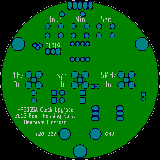
In real world it is 79.5 mm in diameter.
This is the solder side, three buttons, three SMB jacks and two pins for power will be mounted on this side, facing into the instrument.
Optionally the “T|R|G” pins can be populated and used for in-circuit-programming, with a 3.3V or 5V async port.
The TXD and RXD pins double as the Sync input and PPS Output, so in theory you could also use those for ISP purposes.
I managed to make this side one unbroken ground-plane.
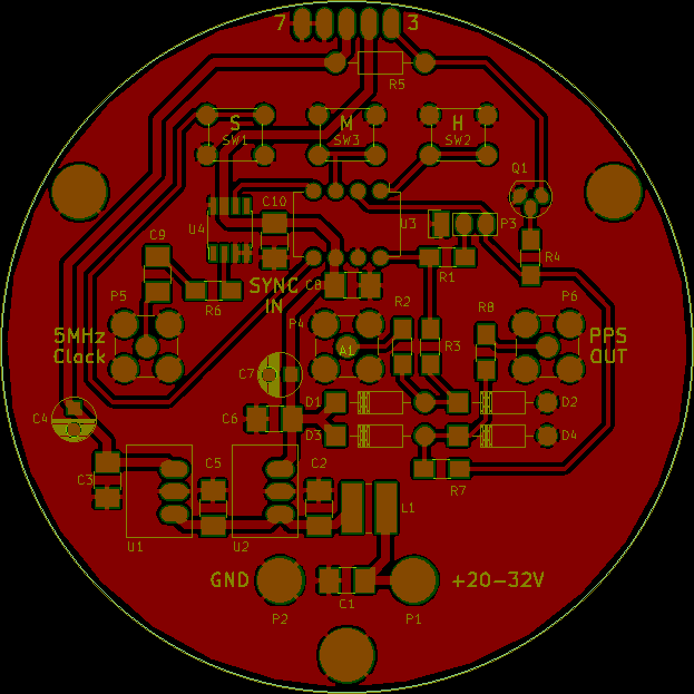
The component side will be mounted towards the LED board (A19A2). I used a lot of surface mount components because this is the Century of the Fruitbat, but also a few through-hole components to match what I happen to have in stock, and in one case to make the PCB layout easier.
This is the first KICAD layout I have sent to production, and it hasn’t made me hate KICAD, so there’s that.
Software
The software will be pretty trivial, and I’m hacking a bit on that while I wait for the PCBs to arrive.
Here’s the plan:
Under normal circumstances the “SCTimer/PWM” section of the ARM chip sends a pulse to the MM5313 chip every second, stepping the clock forward.
Pressing the ‘Hour’ button will send 3600 extra pulses to the MM5313 chip, stepping the clock one hour forward.
Pressing the ‘Min’ button will send 60 extra pulses to the MM5313 chip, stepping the clock one minute forward.
Pressing the ‘Sec’ button will send an extra pulse to the MM5313 chip, stepping the clock one second forward.
If the ‘Sec’ button is held for more than 200 ms, the clock is stopped, and it will start again either when the ‘Sec’ button is released or on the third good 1Hz low->high transition on the ‘Sync Input’.
I’m not starting the software from scratch, I’m using Kevin Townsends LPC810_Codebase github project.
The CLKIN/ISP boot loader entry foobar
NXP mapped both the ISP/boot loader entry and the CLKIN functionality to the same pin - when there are only 8 pins something has to give.
The problem with that is that you cannot have both at the same time.
Either you disable the ISP/boot loader entry and risk bricking your chip because you cannot reprogram it, or the 5 MHz clock will have to be synchronized to the internal RC oscillator clock, which introduces jitter.
For the LED clock that jitter obviously doesn’t matter, it’s a multiplexed display anyway.
But if you plan to use the PPS output, 33⅓ ns jitter will be annoying.
I decided to play it safe and retain the ISP/boot loader entry.
To get rid of the jitter:
Surgically swap pin 4 and 5 on the LPC810 (U3), and program the magic flash location to disable the ISP/boot loader functionality.
Have the software start on internal clock, check on startup if the ‘Sec’ button is pressed, and if so call into boot loader.
Sanity check the CLKIN signal, and if it looks good reconfigure the chips system clock to use it.
Shouldn’t be too hard, but time will show if I care enough to do it.
Availability
All of this is/will be open source under the beerware license.
I have ordered 10 PCBs from SeeedStudio and the surplus will be donated to nice homes when I have got my HP5065A working.
phk